


If you are working with thin films, epitaxial layers, or single crystal materials, you have probably asked yourself this question at some point: what is phi scan in XRD? It is a fair question too, because the way crystals arrange themselves in space, especially in the in-plane direction, has a direct say in electrical, optical, and mechanical performance.
Before we get into the details of Phi scanning, it helps to have a handle on basic XRD working principles. That way, you can better appreciate how this technique differs from other scan modes. Identifying a crystalline phase through routine qualitative analysis is really only step one. The real challenge often lies in assessing in-plane alignment, something a conventional symmetric scan simply cannot see. A standard 2θ-ω scan gives you out-plane crystal information, meaning planes parallel to the sample surface. But it is essentially blind to the symmetry and orientation distribution that runs parallel to the surface. So if you want to get a handle on in-plane texture, epitaxial relationships, or rotated domains, understanding Phi scanning gives you a precise and practical way to do that.
What Is Phi Scan in XRD?
Put simply, a Phi scan in XRD is a rotational diffraction measurement. It is specifically designed to evaluate in-plane crystal orientation and symmetry.
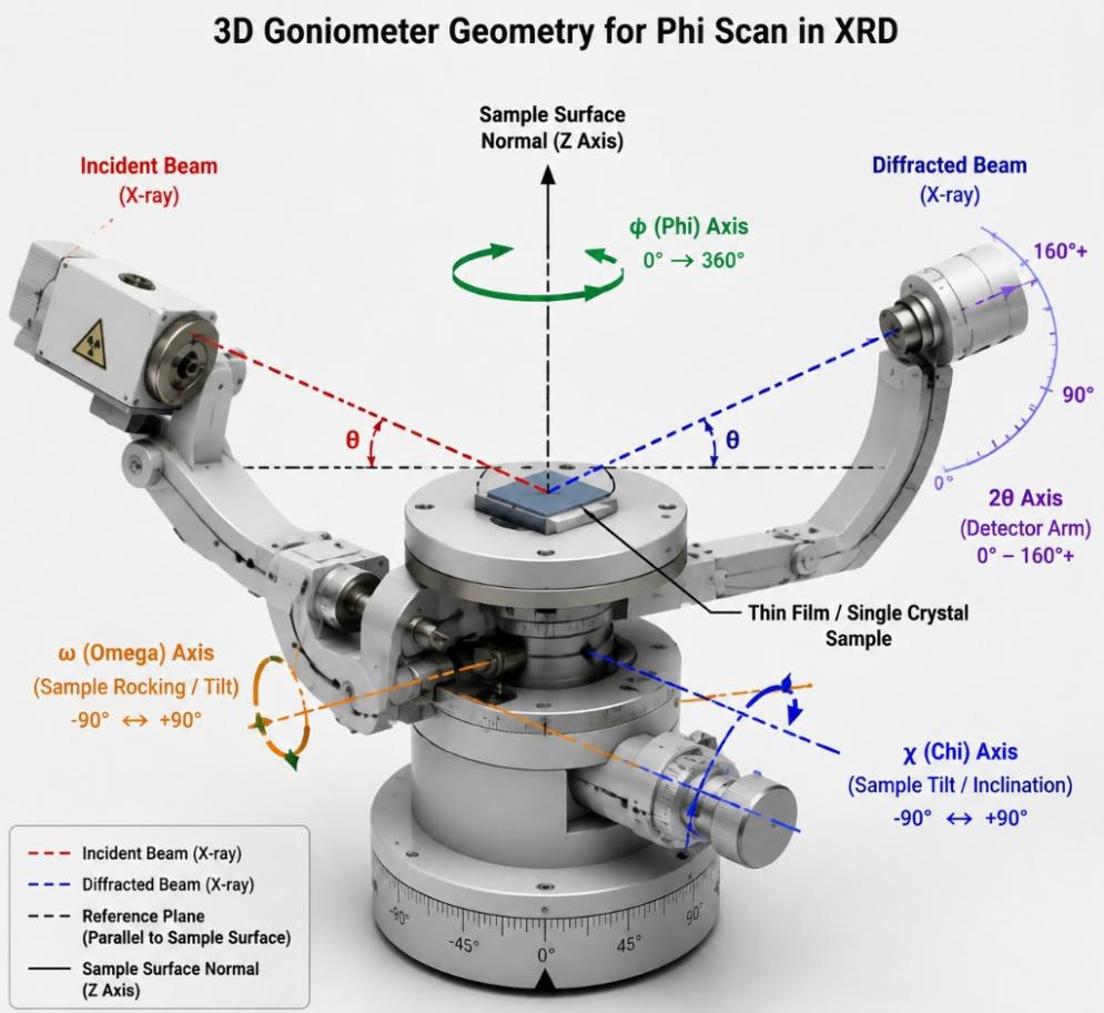
In crystallographic analysis, the Phi scan (φ Scan) falls under the category of asymmetric X-ray diffraction techniques. The sample rotates a full 360° around its surface normal axis, which is the φ axis. This rotation is what allows you to peer into the in-plane crystal structure.
In a regular symmetric XRD setup, like a 2θ-ω scan, the geometry mainly catches planes that sit parallel to the sample surface. You get the out-plane spacing, sure, but the full in-plane orientation relationship remains hidden. That is where Phi scanning steps in. Here, you lock the diffraction angle (2θ) and tilt angle for a specific off-axis (asymmetric) reflection. Then you simply spin the sample around its own central normal axis, the φ axis, and record what happens. The technique is very common in the semiconductor wafer world, functional coatings, and single crystal substrate evaluations where in-plane alignment, lattice matching, and domain structures really matter.
How Does Phi Scan Work in XRD?
Phi Scan Measurement Principle
The underlying principle of a Phi scan relies on picking an asymmetric crystal plane as your target. That simply means a plane that sits at a known tilt angle relative to the physical sample surface.
If you were to pick a plane that is perfectly parallel to the surface, rotating the sample 360° around the surface normal would only produce a flat, constant baseline intensity. There would be no variation to capture. So instead, you tilt the sample using the χ axis or the ψ axis, depending on your diffractometer’s geometry. This tilt is set to a specific angle that brings that asymmetric plane into play.
Now, as the sample rotates around the φ axis, diffraction peaks will only show up at certain rotational positions. That happens when the asymmetric plane in question satisfies Bragg’s Law (nλ = 2d sinθ). So as you sweep through the full 360°, you plot the intensity peaks against the rotation angle. That plot becomes a visual fingerprint of the material’s rotational symmetry.
Key Information Revealed by Phi Scan
When you run a Phi scan properly, it gives you a few critical pieces of crystallographic information. Here is what you can extract:
- In–Plane Crystal Symmetry: The number of peaks you see and their angular spacing tell you the fundamental rotational symmetry of the crystal.
- In–Plane Preferred Orientation / Texture: If the peaks are sharp and narrow, that means your material is highly oriented or epitaxial. Broad peaks or a flat continuous signal, on the other hand, usually point to a random grain orientation distribution.
- Epitaxial Relationship: Overlay the Phi scan pattern of a thin film with the pattern from the underlying substrate. The offset between their peaks tells you if the film lattice grew in registry with the substrate lattice.
- Domain and Twinning Structures: Extra peaks or unexpected peaks at non-standard angles often signal the presence of rotated domains, anti-phase boundaries, or twinning defects inside the material.
- Foundation for Pole Figures: If you collect Phi scan data at multiple tilt angles (χ), you get the raw dataset needed to build pole figures and orientation distribution functions (ODF). That is where you move from 1D to 2D texture analysis.
Schematic showing the relationship between a 1D XRD phi scan and a 2D pole figure for cubic (111) thin films with 180-degree twin domains
Phi Scan vs Other XRD Scans: What Is the Difference?
To help you pick the right scan mode for your analysis, here is a quick comparison of Phi scanning against the other main XRD scan types.
| Scan Mode | Main Purpose | Key Information Revealed |
| θ-2θ Scan | Phase ID and out-plane analysis | Crystalline phases, out-plane spacing, d-values |
| Omega (ω) Scan | Crystalline quality and defects | FWHM of rocking curve, dislocation density, mosaic spread |
| Phi (φ) Scan | In-plane texture and orientation | In-plane symmetry, lattice alignment, epitaxy |
A rocking curve (Omega scan) looks at structural perfection perpendicular to the surface. But the Phi scan is specifically designed to analyze grain arrangement and rotational symmetry in the horizontal direction. They complement each other, but they answer different questions.
How to Perform a Phi Scan Measurement Step by Step
Getting reliable Phi scan data is not something you can rush. It takes systematic calibration and precise geometry setup. Here is a step-by-step breakdown of the standard measurement routine.
Step 1: Mount and Center the Sample. You start by fixing your thin film or single crystal sample onto the goniometer stage. Proper centering matters a lot here, as emphasized in proper XRD sample preparation. You need to align the physical center of the sample surface with the instrument’s rotation center. That Z-axis alignment is critical, otherwise you will get eccentric wobble as the sample spins, and that will distort your data.
Step 2: Identify an Asymmetric Target Plane. Next, you calculate and select a suitable asymmetric plane (hkl). It needs to have decent diffraction intensity and a known tilt angle (χ) relative to the surface plane.
Step 3: Align the XRD System. Now you dial in the 2θ and ω angles to match the theoretical position of that target plane. Tilt the goniometer to the required χ angle. Then do a fine optimization to maximize the diffraction peak intensity. Good alignment at this stage is what separates clean Phi scan data from noisy, uninterpretable results.
Step 4: Execute the 360° Phi Scan. Finally, you set the φ axis to rotate continuously from 0° to 360°. Step size is an important choice here, typically between 0.1° and 0.5°. The instrument records diffraction intensity at each step along the way.
How to Read and Analyze Phi Scan Results
Interpreting Peak Count and Symmetry
When you look at a Phi scan pattern, you are essentially reading the x-axis from 0° to 360°. The positions of the peaks, their number, and their full width at half maximum (FWHM) all tell a story.
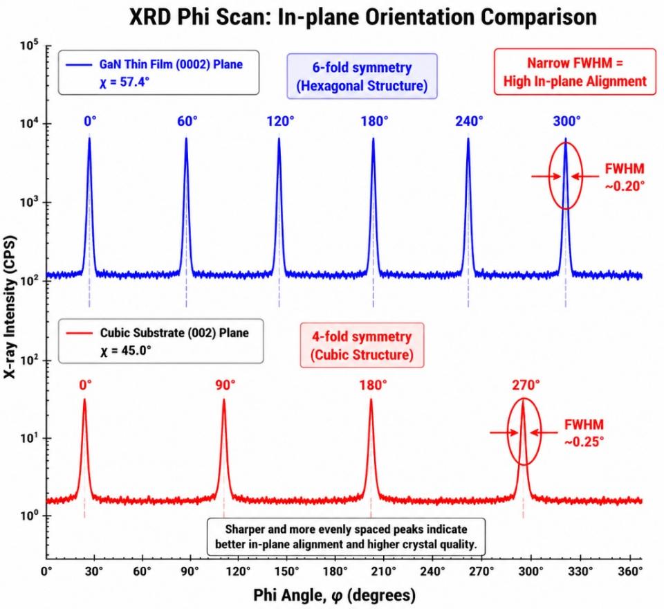
Peak count and lattice symmetry: Take a cubic crystal with a (001) orientation and pick an asymmetric reflection. As you rotate a full circle, you might see four peaks spaced 90° apart. For a hexagonal film like GaN, measured on an asymmetric plane, you typically get six clear peaks with 60° spacing. So the number of peaks directly reflects the rotational symmetry of your crystal.
Peak width and texture quality: The sharpness of each Phi peak, quantified by the FWHM, gives you a measure of in-plane orientation spread. Narrower peaks mean higher crystalline quality and less rotational scatter among the grains.
Evaluating Epitaxial Lattice Mismatch
If you are working with heterostructures, comparing the Phi scan peaks from the film and the substrate tells you a lot about the growth mechanism.
Direct Epitaxy: The film peaks line up exactly with the substrate peaks, meaning a relative offset of 0°. That confirms the film has the same in-plane crystallographic orientation as the substrate.
Rotational Epitaxy: The film peaks show a systematic angular shift relative to the substrate peaks, say 30° or 45°. This usually points to domain-matched epitaxy, where the film lattice rotates to release interfacial strain.
Applications of Phi Scan in Materials Science and Industry
As a core part of broad XRD applications in material analysis, Phi scanning plays an important role in several high-precision fields.
Thin Film and Epitaxial Electronics
In compound semiconductor manufacturing, think GaN, SiC, GaAs, and also in oxide electronics, Phi scanning is a standard evaluation tool. It makes sure the functional layers you deposit actually have the required crystal orientation, which in turn helps you get the best carrier mobility and device performance.
Semiconductor Wafer Orientation Analysis
In wafer processing and quality control, Phi scanning helps pinpoint the exact crystallographic orientation of substrates and epitaxial layers. By verifying the wafer’s correct crystal direction and in-plane uniformity, engineers can fine-tune processing conditions. That directly translates to better device consistency and overall performance.
Industrial Quality Control and R&D
In a production environment, Phi scanning supports process validation for commercial semiconductor wafers, optical coatings, and functional thin films. R&D teams rely on it to verify film uniformity, monitor batch-to-batch reproducibility, and catch structural defects that might arise from temperature shifts or stress variations.
Single Crystal Characterization
Before deposition even starts, you can use Phi scanning to verify the physical orientation of cut single crystal substrates like sapphire, STO, or silicon wafers. It confirms that the substrate surface matches the specified crystallographic cut.
Phi Scan Requirements: What XRD Equipment Do You Need?
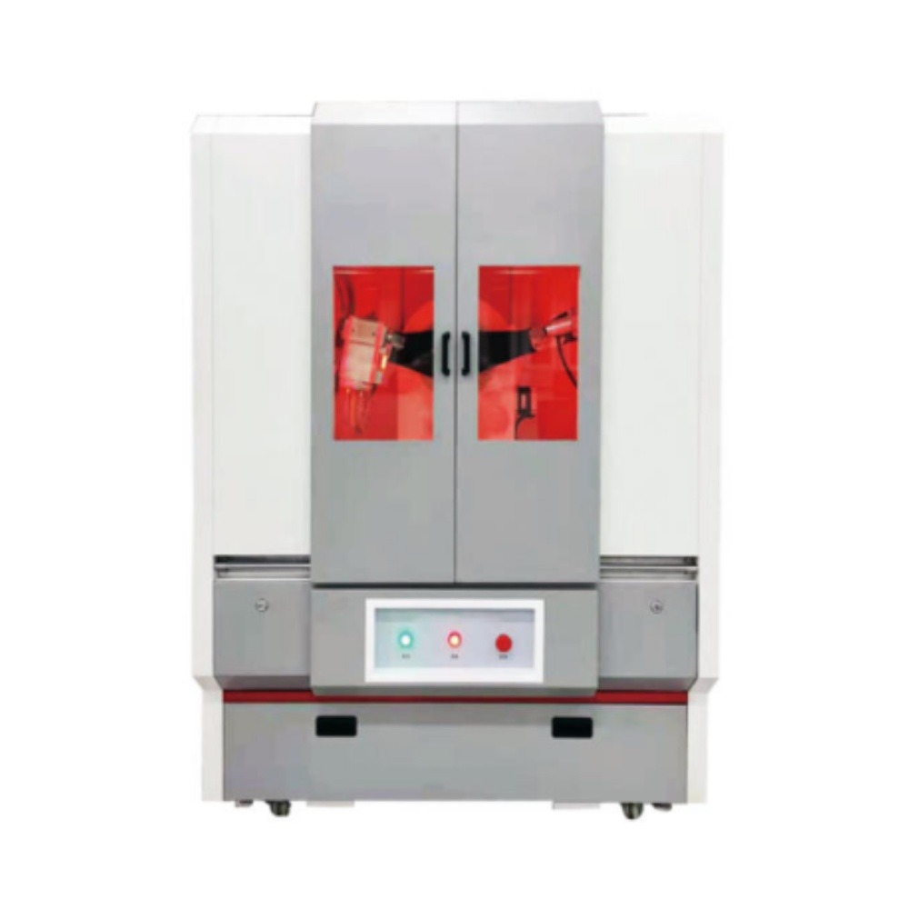
If your lab runs Phi scans on a regular basis, you need to think carefully when choosing an X–ray diffractometer (XRD). Systems with flexible goniometer configurations and modular hardware make your life much easier.
A standard two-axis powder diffractometer does not have the necessary rotational degrees of freedom. For full texture and in-plane orientation analysis, you typically need a more advanced multi-axis system.
4–Circle Goniometer / Eulerian Cradle: The system must have independently controlled φ (azimuth) and χ (tilt) motorized axes. That is non-negotiable, because you need to position the sample for off-axis diffraction conditions.
Parallel Beam Optics: Adding an X-ray mirror or a Ge monochromator helps reduce beam divergence. That minimizes peak broadening and improves the signal-to-noise ratio for thin film samples.
Integrated Texture Analysis Software: Good software simplifies the whole workflow, from peak-fitting to pole figure visualization and ODF construction.
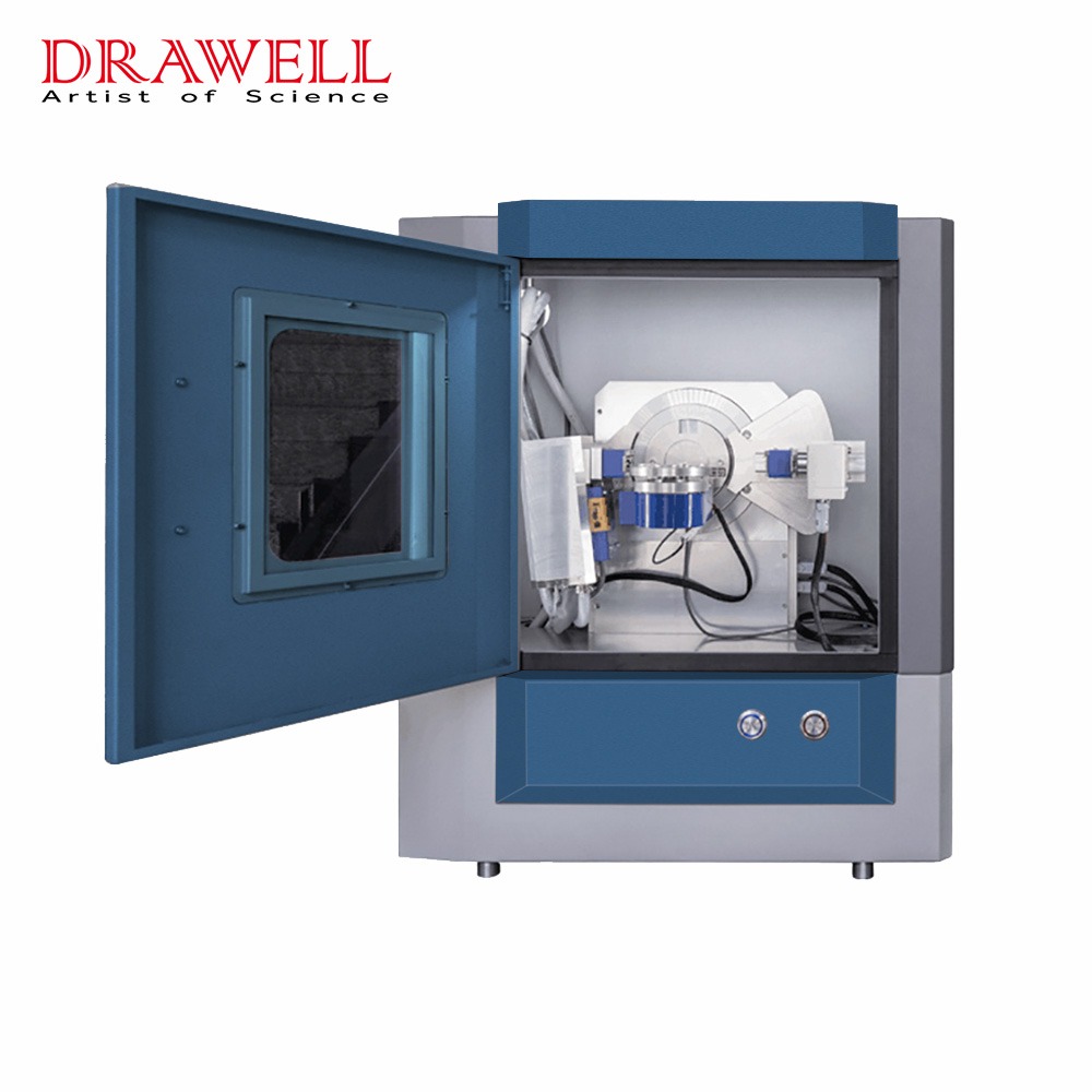
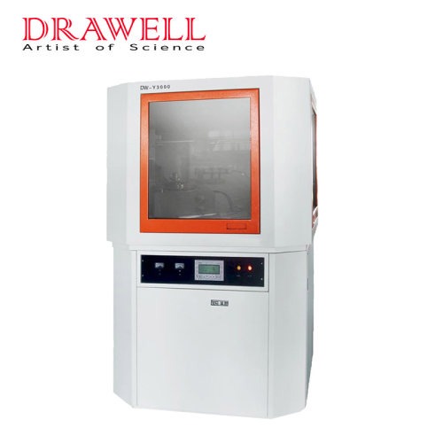
For labs looking for a system that can handle Phi scans, Drawell offers modular diffraction solutions with flexible goniometer configurations. These setups let research groups and industrial QA labs run routine phase ID and high-precision in-plane texture mapping on the same platform.
Common Issues and Troubleshooting in Phi Scanning
Sometimes things do not go smoothly. Here are a few common problems and practical fixes.
Issue 1: No Diffraction Peaks Detected
Possible causes: The χ tilt angle might be miscalculated. Your 2θ-ω positioning could be off. Or maybe the sample height (Z-axis centering) was never properly calibrated.
Fixes: Re-calibrate the sample Z height. Run a fine 2θ-ω coupled scan to lock onto the actual Bragg peak position. Double-check your tilt angle calculation.
Issue 2: Exceptionally Low Peak Intensity
Possible causes: The asymmetric plane you picked has a weak scattering factor. Or your film is extremely thin, maybe below 10 nm.
Fixes: Choose an asymmetric plane with a higher structure factor. Increase the dwell time per step. Or switch to a parallel beam optics configuration to boost signal.
Issue 3: Asymmetrical Peak Heights or Shapes
Possible causes: The sample’s physical center might be offset from the rotation center, causing eccentric wobble. Or the sample surface could have non-uniform strain.
Fixes: Re-center the sample using optical or laser alignment tools to eliminate the wobble.
Phi Scan vs Pole Figure: What Is the Relationship?
People often mention Phi scan and pole figure in the same breath, but they are not the same thing. A Phi scan is essentially a 1D data slice, whereas a pole figure gives you a full 2D or even 3D mapping of crystal orientation.
A Phi scan is recorded at a single fixed tilt angle (χ). You just rotate the sample 360° and capture the intensity curve.
A pole figure is built by collecting multiple Phi scans at a series of tilt angles, for instance stepping χ from 0° to 85° in 5° increments. Then you map those intensity data onto a stereographic projection.
For a quick check of symmetry and lattice alignment, a single Phi scan often does the job. For a comprehensive quantitative texture assessment across the entire orientation space, you need the full pole figure dataset.
Final Thoughts
Once you get a good grasp of what is phi scan in XRD, you open up a whole new layer of analysis beyond simple phase identification. You start to see the details of in-plane crystal arrangement, how grains are aligned, and how domains are rotated. Whether you are optimizing a thin film deposition process or verifying a single crystal substrate, a multi-axis XRD system gives you the quantitative data you need for advanced materials research and reliable quality control.
Get Quote Here!
Latest Posts



What Next?
For more information, or to arrange an equipment demonstration, please visit our dedicated Product Homepage or contact one of our Product Managers.


