

In the semiconductor industry, Raman spectrometers can assist the industry in studying the fundamental properties of semiconductor materials. Semiconductors containing single elements, such as silicon (Si), germanium (Ge), and semiconductors composed of multiple components, such as zinc selenium (ZnSe) and gallium arsenide (GaAs) semiconductors. In the material manufacturing stage, the characteristics of these semiconductor materials will determine the quality of the subsequent wafer manufacturing and IC packaging processes. This stage is the most crucial step.

In the process of wafer manufacturing, using a Raman spectrometer as a tool for process analysis and quality control will help to improve the quality of products, increase the yield rate and thus increase the overall yield.
Typical applications of Raman spectrometers in the semiconductor industry today include:
- Material purity;
- Identification of contaminants;
- Alloy composition;
- Superlattice structure;
- Characteristic factors of intrinsic stress & strain;
- Defect analysis;
- Semiconductor heterostructures;
- Doping Effects of Heterojunctions.
What is ZnSe?
ZnSe is a typical II-VI semiconductor material with a zinc blend structure and a direct band gap. The forbidden bandwidth at room temperature (300K) is 2.698eV, and at low temperature (<10K), its forbidden bandwidth is 2.821ev, corresponding to blue light with a wavelength of 459.4nm.
Application and Research of ZnSe
Thermal evaporation of ZnSe powder in a high vacuum has been applied. ZnSe monolayers with thicknesses between 30 nm and 1 µm were deposited on c-Si and glass substrates at room temperature.
In addition, SiOx/ZnSe periodic multilayer films prepared by the same deposition technique were investigated with ZnSe layer thicknesses of 2 and 4 nm. Raman spectra were measured at 295K using the 442nm line of the He-Cd laser and different lines of the Ar+ or Ar+/Kr+ laser. The observed Raman signatures are related to multiple optical phonon (1LO to 4LO) light scattering and randomly oriented crystalline ZnSe grains of ZnSe monolayers and multilayers.
Relatively large line widths (≈15 cm-1) of the 1LO band have been observed, which are associated with lattice distortions in the grains and the presence of amorphous phases in layers thinner than 100 nm.
The Behavior of ZnSe in Raman Analysis
All measurements in the experiments were performed in air at room temperature. All spectra plotted on the same graph are scaled the same.
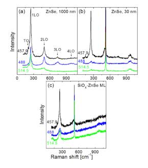
The upper panels represent the Raman spectra of 1 µm (a) and 30 nm (b) ZnSe monolayers and SiOx (4 nm)/ZnSe (4 nm) multilayers (c) measured under three laser excitations.
Figure 1a shows three Raman spectra of a ZnSe layer with a thickness of 1 µm deposited on a Corning 7059 glass substrate. Better resolution is obtained at excitation conditions close to the resonance Raman scattering conditions.
The most muscular enhancement of the Raman signal is observed when the excitation light is close to the material’s optical bandgap Eg0. Since the 1LO band is the densest in the Raman spectrum excited by the 457.9 nm line, the energy of this line should be close to the optical band gap.
This is consistent with previous results showing that for the optical bandgap of a 1-µm-thick ZnSe layer, the optical absorption follows the laws of directly allowed electronic transitions in crystalline semiconductors.
Figures b and c show the Raman spectra of the ZnSe layer with a thickness of 30 nm and the SiOx(4nm)/ZnSe(4nm) multilayer, respectively.
Both samples were deposited on the c-Si substrate, and the observed narrow solid band peaked at 521 cm-1 due to scattering from the substrate. The 1LOZnSe band intensity increases with decreasing excitation wavelength, and a series of 4 peaks can be seen only in the spectrum excited by the 457.9 nm line.
In practice, however, SiOx/ZnSeML (with various thicknesses between 2 and 10 nm) were characterized by Raman spectroscopy using the 442 nm line, showing resonance behavior in the Raman spectrum. It is related to the size-induced variation of the bandgap energy with layer thickness.
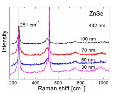
Above are the Raman spectra of ZnSe monolayers of four different thicknesses (shown) measured using 442 nm excitation light.
It depicts the Raman spectra of a series of ZnSe monolayers with thicknesses between 30 and 100 nm measured using a 442 nm laser line. The intensity of the 1LO band of the 30 nm layer is significantly higher than that of the other samples. The Raman results show that the ZnSe layer with a thickness of less than 50 nm can show good chemical sensitivity due to the small grain size.
Summarize
Using stepwise thermal vacuum evaporation, the application of Raman spectroscopy for structural characterization of thin and ultrathin ZnSe layers deposited at room temperature. Measurements under excitation with three different Ar+ laser lines show that the 1LO band intensity leads to a maximum when excited with the 457.9 nm line, independent of layer thickness.
Measurements with the 442 nm line show that its energy is closer to the optical band gap of the grains in the thinnest monolayer and the ZnSe layer in the ML than that of the 457.9 nm line. This observation indicates carrier confinement and implies that the grain size in these layers is about 10 nm.